Opt System 100 Pecvd Photo
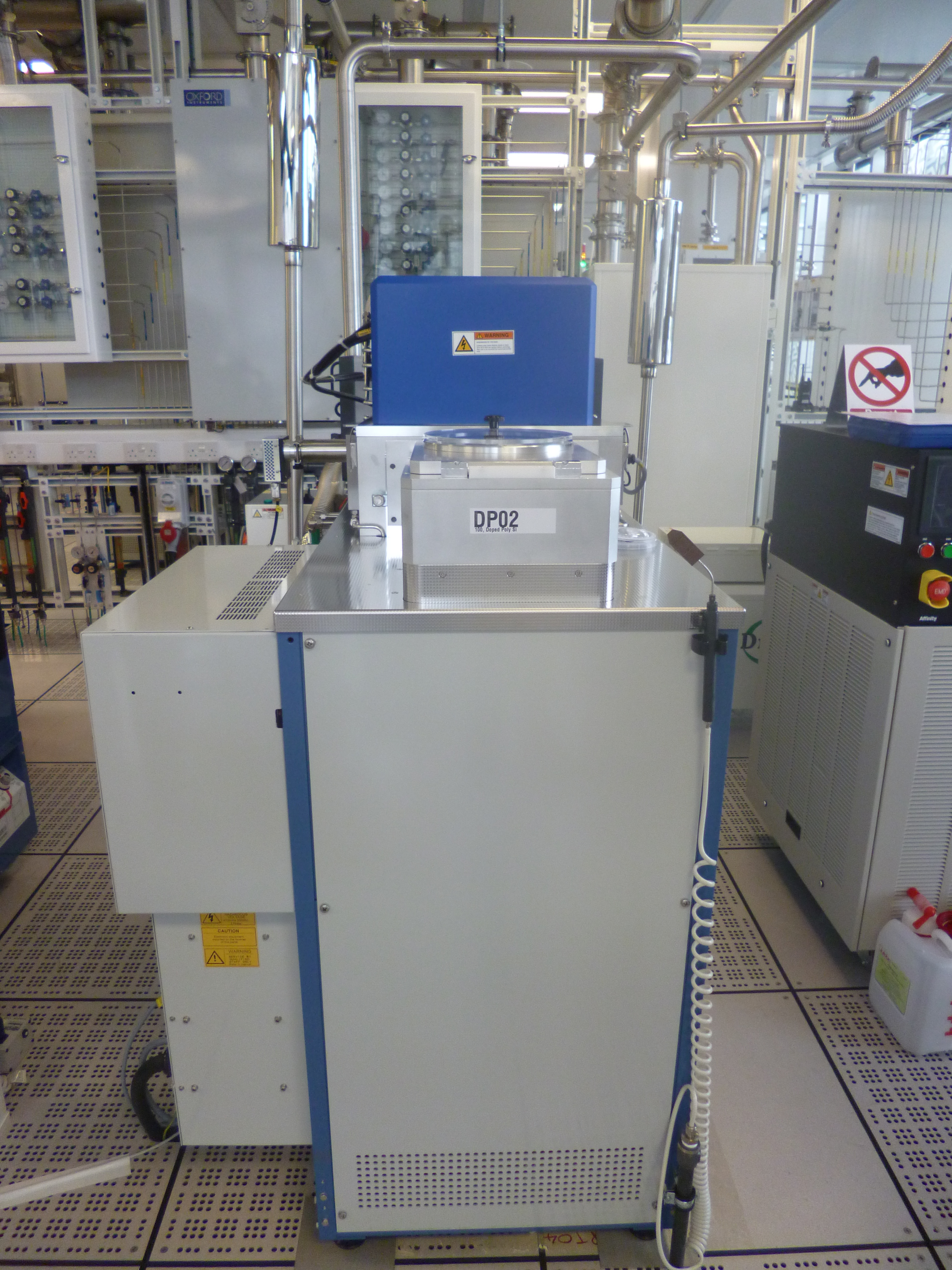
Plasma Enhanced Chemical Vapour Deposition (PECVD) system for the growth of amorphous and polycrystalline Si, SiGe and Ge layers. The layers can be doped during growth either n-type (using PH3) or p-type (using B2H6), thereby allowing p-n junctions to be formed. Amorphous silicon uses SiH4 for the source of silicon and CF4 & O2 for cleaning. The growth temperature is typically 250C, giving a growth rate of around 25 nm/min. Stress in the deposited layer is typically <200Mpa. Polycrystalline silicon uses SiH4 for the source of silicon and CF4 & O2 for cleaning. The growth temperature is typically >=610C. The growth rate at 610C is ~2 nm/min and at 650C ~ 20nm/min. Microcrystalline silicon uses SiH4 for the source of silicon and CF4 & O2 for cleaning. The growth temperature is typically in the range 585 - 610C, giving growth rates in the range 1 - 2 nm/min. Amorphous and polycrystalline germanium use GeH4 as a source of Ge and CF4 & O2 for cleaning.
LESSEY, MARK
You can download the raw data used to create this page:
The following open datasets were used to build this page:
© 2025 University of Southampton

