MA6 Mask Aligner Photo
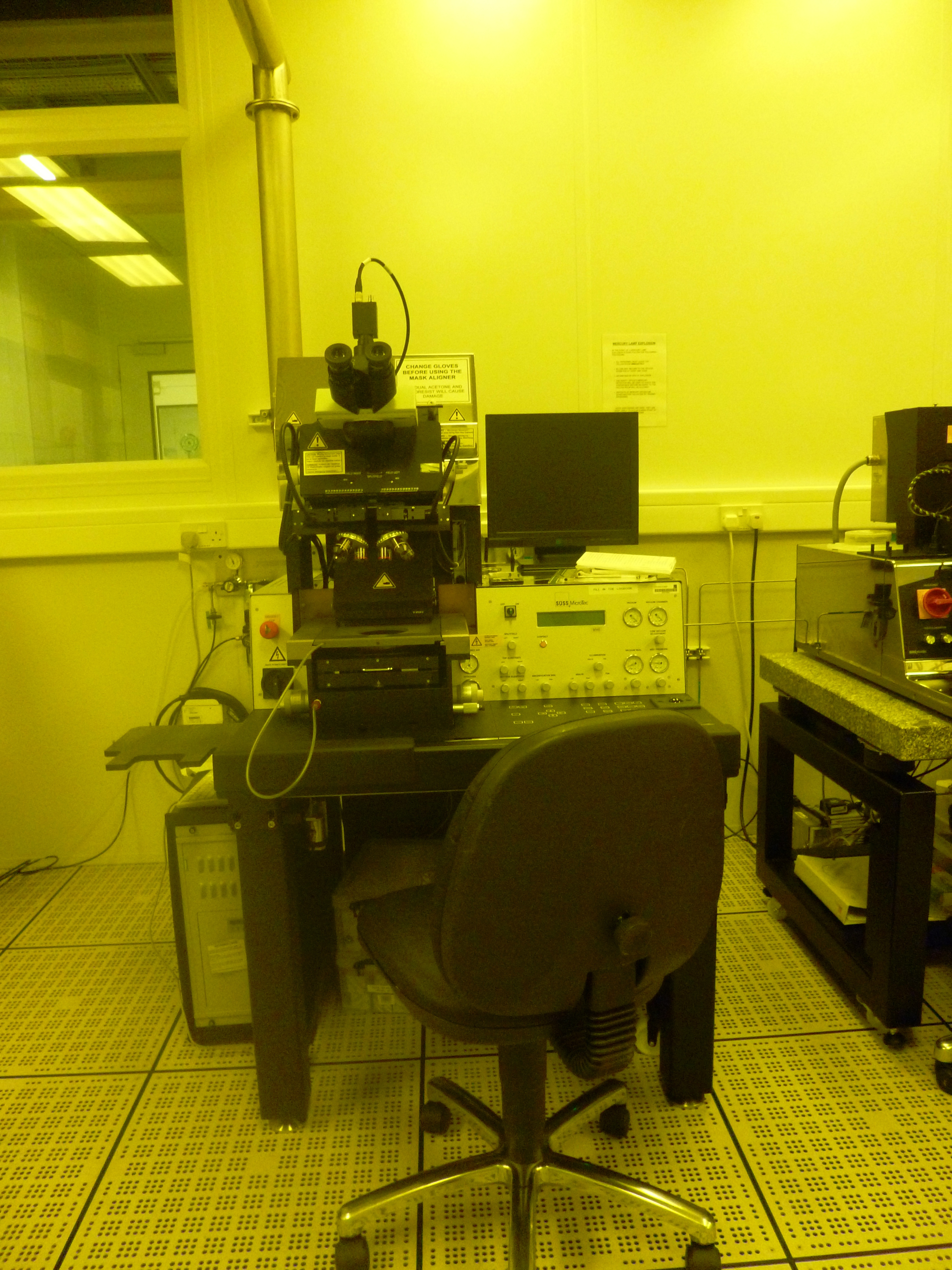
Allows printing of structures on flat substrates by replication of a mask using photoresist exposure and development followed by etching, for example. Feature sizes below 1 micron may be replicated over wafers up to 100mm diameter. Double-sided aligning allows alignment of features on both sides of a silicon wafer
SESSIONS, NEIL
You can download the raw data used to create this page:
The following open datasets were used to build this page:
© 2025 University of Southampton

